An Introduction To The PCB Manufacturing Process
Printed Circuit Boards (PCBs) serve as the backbone of electronic devices, establishing a foundation for seamless connectivity and optimal functionality. With Horizon, we will delve into the intricate realm of PCB manufacturing, where we will unravel the essential processes that underpin this crucial aspect of electronic design and assembly.
What is PCB Manufacturing?
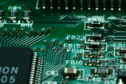
Printed circuit boards (PCBs) form the backbone of all major electronics. They tell the electricity where to go and essentially bring your electronics to life. They direct current around their surface through a network of copper pathways. The PCB manufacturing process requires a complex procedure to ensure the performance of the finished product. The number of steps required depends on the complexity of the PCB itself.
PCB Manufacturing Process
1. Design and output
PCB manufacturing commences with a comprehensive plan, where the designer meticulously lays out the blueprint to meet specified requirements. After encoding the PCB design blueprint, it undergoes examination by the designer before being sent for fabrication. This crucial step is referred to as the Design for Manufacture (DFM) check, a pre-fabrication procedure ensuring the integrity of the circuit board design.
2. Design review and engineering
Prior to fabrication, a thorough review of the design is conducted to identify potential errors and confirm the absence of missing components or incorrect structures. Carried out by the engineer, this meticulous examination scrutinises every aspect of the PCB design before progressing to the printing phase.
3. Printing the PCB design
Following the completion of all checks, the PCB design is printed to visually represent the board’s details and layers. Clear ink highlights non-conductive parts, such as the fibreglass base, while black ink delineates conductive copper traces and PCB circuits. Once printed, a registration hole is punched through to serve as a guide for aligning the films in subsequent stages of the process.
4. Printing copper for interior layers
This phase marks the actual commencement of PCB manufacturing. A copper foil layer or coating is applied to the laminate material where the PCB design is printed. Subsequently, the copper is pre-bonded to the laminate, establishing the structural foundation for the PCB. The excess copper is then etched away to reveal the design blueprint.
Additionally, a photo-sensitive film covers the laminate panel, containing photo-reactive chemicals that harden upon exposure to UV light. The UV light penetrates the sheer parts of the film, revealing the copper pathways. Following this, the bare board undergoes a thorough wash with an alkaline solution and pressure cleaning to eliminate excess photoresist. Finally, the board is left to dry.
5. Etch the inner layers or core to remove copper
In the final step, the elimination of any undesired copper on the core or inner layers of the PCB is executed. This involves covering the necessary copper on the PCB panel and applying a chemical solution to the remaining areas, causing it to etch away the unwanted copper. This chemical etching process effectively eliminates all unprotected copper from the PCB.
6. Layer alignment
Drilled holes serve to align the inner and outer layers with the assistance of an optical punch machine. Subsequently, a separate machine inspects the board to ensure error-free alignment and overall integrity of the PCB.
7. Automated optical inspection
Following the optical punch, a meticulous optical inspection is carried out on the PCB to verify its defect-free status. Once the PCB successfully passes this inspection, it is cleared to proceed to the subsequent steps of the manufacturing process.
8. PCB layers lamination
The PCB laminating process comprises lay-up and lamination. During lay-up, the layers are fused, incorporating a substrate layer over the prepreg resin. Another copper layer is applied and pressed together with the existing layers. Pins are punched through the layers to ensure alignment and secure bonding. Subsequently, the PCB undergoes lamination, involving the application of heat and pressure to fuse the layers seamlessly, facilitating the easy removal of the PCB.
9. Drilling
Registration holes are drilled to secure the PCB in place before the actual holes are drilled. A computer-guided drilling machine then creates holes to expose the substrate and inner panels. Any residual copper is removed once the drilling process is complete.
10. PCB plating
A chemical solution is applied to fuse all the PCB layers, and the board undergoes cleaning and bathing. Additionally, the chemicals coat the panel with a thin layer of copper, seamlessly flowing into the drilled holes from the topmost layer.
11. Outer layer imaging
The outer layer of the board undergoes an additional application of photoresist, after which the board is subjected to imaging, where UV lights harden the photoresist. Following this process, the outer layer is plated with a thin copper layer and receives an additional thin layer of tin to safeguard the copper on the outer layer.
12. Outer layer etching
The tin guard introduced in step 11 serves as protection for the required copper from the chemical solution used during etching. Once all residual copper and resist have been removed, the layer is prepared for inspection.
13. Outer layer automated optical inspection
Automated optical inspection (AOI) is similarly performed for the outer layer, mirroring the process applied to the inner layer. This meticulous examination guarantees that the layer conforms to the design specifications and is free from any detrimental copper remnants that could result in defects on the circuit board.
14. Solder mask application
An ink epoxy and solder mask film are applied to each panel. The UV light concentration indicates areas where the solder mask needs removal, and the necessary solder mask is baked onto the board. This solder mask imparts the green colour commonly seen on circuit boards and serves to protect them from oxidation and corrosion.
15. Silkscreen application and surface finish application
In the silkscreen application phase, crucial information such as warning labels, part numbers, company ID numbers, and the manufacturer’s logo is directly printed onto the board. Subsequently, the PCB undergoes surface finish application.
16. PCB finishing
In this step, the board’s surface is plated with conductive materials to establish a reliable connection between the PCB and electronic components. The surface is then finished to provide a solderable surface, safeguarding any exposed copper from oxidation caused by air exposure.
17. Electrical reliability test
Electrical tests are conducted on various sections of the board to verify that it meets the required functionality. The tests include:
- Circuit continuity test: Identifies any disconnections in the PCB.
- Circuit isolation test: Examines the circuitry for shorts.
- ‘Bed of nails’ test: Assesses how well the board tolerates high-pressure contact at its test points.
- Flying probe test: Checks electrical contacts and verifies the electrical connectivity of the circuit board.
18. Profiling and route out
The fabricator identifies the shape and size of each individually printed circuit board cut from the construction board. Routing out is employed to facilitate the separation of the boards in the circuit board assembly.
19. Quality check and visual inspection
The board undergoes inspections and quality checks to ensure the final PCB product is free from defects. This encompasses verifying correct hole sizes, adhering to design specifications for board dimensions, ensuring finished boards lack sharp edges, and confirming boards are free from any debris.
20. Packaging and delivery
This marks the final stage of the PCB manufacturing and assembly process. PCBs are coated with a sealing material to prevent dust ingress. Sealed boards are then placed into containers that shield them from damage during shipping and delivery.
Horizon is your trusted partner
In the ever-evolving landscape of technology, PCB manufacturing undergoes continuous advancements. Grasping the intricacies of PCB production is crucial for engineers, designers, and enthusiasts. This guide serves as a comprehensive introduction, covering everything you need to know about PCB manufacturing.
At Horizon Electronics, we not only provide this valuable insight but also manufacture an extensive range of cable assemblies and serve as a wholesale distributor of electrical connectors for PCBs.
Our provisions focus on end-to-end solutions for our PCB services – from products R&D and prototyping to full scale production with electronic PCB assembly services, going beyond what the average assembly PCB company will do.
Our team of engineers use Altium Automation Software to design our products, from the simplest to the most complex PCB’s. From prototype to production stages, our PCB assembly factory in Taiwan offers us low-cost solutions, quick turnaround and world standard product quality.
Contact us today, and our team will be delighted to assist you.


